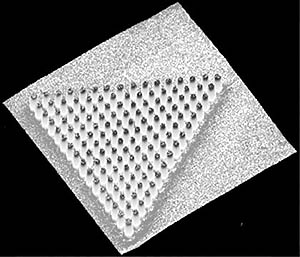
Pillars in perfect order
|
|
|
|
|
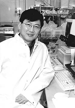
Stephen Chou (Photo by Denise
Applewhite)
|
By Steven Schultz
In the world of Stephen Chou, J.C. Elgin Professor of Engineering, a speck of dust can be enormous.
For a man who routinely creates objects that are measured in billionths of meters, specks that are just visible to the naked eye--or even to a common microscope--are like boulders on the beach.
So it's fitting that one autumn day in 1997, a speck of dust changed Chou's world.
In Chou's NanoStructures Lab at the University of Minnesota, graduate student Lei Zhuang was experimenting with a technique Chou had discovered for making ultrasmall plastic structures by stamping them out of soft plastic. In one experiment, dust crept into the space between the stamp and the plastic, preventing the two from coming together. Later, when Zhuang looked at the plastic, he saw that it had a minute, perfectly ordered pattern, even though the two parts had never touched each other.
It turned out Chou and Zhuang had stumbled on an entirely new technique, a way to coax the structures to assemble themselves. Suddenly, the hard-to-make stamp, called a mask, was no longer necessary. "Here the polymer will form itself, without a mask. It's really wonderful," says Chou.
And it's more than just a neat trick. The discovery has yielded surprising insights into the behavior of materials at very small scales, while raising a host of basic research questions. Chou also believes it could pave the way to a new generation of products, from video displays and miniature electronics to devices for sorting DNA molecules.
National, international patents
Chou, who came to Princeton in January 1998, has dubbed the technique LISA, for Lithographically Induced Self Assembly. Princeton has filed for US and international patents on the process, which Chou first described at the International Symposium on Cluster and Nanostructure Interfaces in October. He expects to publish the discovery in the December issue of the Journal of Vacuum Science and Technology.
|
|
|
|
|
|
But these pillars are far from the smallest things Chou has created, and the LISA technique is only one of many discoveries Chou has made in the field of nanofabrication. Princeton recruited him from the University of Minnesota as part of a major investment in that discipline. In addition to building lab space for Chou and moving all his equipment, the University made an even greater investment in nanofabrication lab space for the entire university through POEM, the Center for Photonics and Optoelectronic Materials.
Nanoimprinting process
Among Chou's many research projects, the one that has attracted the most attention from industry has been his nanoimprinting process, the technique of stamping a template into soft plastic. The technique has yielded structures with features as small as six nanometers, six billionths of a meter. In some materials, that's only a few dozen atoms.
Previously, the only way to make structures that small was a slow and expensive process called electron beam lithography, in which a finely tuned electron beam carves out the desired patterns. Reversing long-held beliefs, Chou discovered that he could accomplish the same thing simply by pressing a template into soft plastic. Making the template is expensive, painstaking work. But once it's done, nanostructures can just be stamped out.
Chou believes that the ease of production will reduce costs more than a thousandfold and will give consumers access to many telecommunications technologies that currently are used only in research labs. Several electronics companies, including IBM, are developing nanoimprint technology.
"There's so much exciting research into nanostructures in the lab," says Chou. "But very few are commercially available. You ask why. The reason is there is no low-cost, high-throughput nanopatterning method. Nano-imprinting is the solution."
In one of his first applications of nanoimprinting, Chou developed a nano-CD, a device that stores the same amount of information as 30 conventional compact disks in the space of a penny. Whereas conventional CDs have grooves more than 800 nanometers in width, nanoimprinting allowed Chou to reduce that size to 10 nanometers.
Quantized magnetic disk
Another product in development is the quantized magnetic disk, a highly compacted version of the material used in computer hard drives or cassette tapes. Conventionally, these devices consist of magnetic particles spread across a thin film. The particles have no natural order, so if bits of data are stored too close together, they tend to erase each other.
Chou used nanoimprinting to replace the flat film with a compact array of minute pillars, thereby invoking an entirely new set of physical laws. Instead of tending toward randomness, the pillars selfmagnetize, locking themselves into only two directions, up or down. The result is that the each pillar can retain its own piece of data even when squeezed against another.
IBM is developing both the nano-CD and the quantized magnetic disk.
In each of these projects, Chou has had to jettison many conventional ideas about the way materials work at very small scales. "As I tell my students, nanotechnology is like going to a new planet. You see new things at every turn."
Pillars--what on earth?
Indeed, the complete novelty of the work has presented teaching challenges. In his first attempts at the University of Minnesota to try nano-imprinting, Chou had difficult convincing his graduate students even to try embossing the tiny features into plastic. "They thought I was crazy," he says.
When they were developing the technique further, Zhuang (who is now at Princeton) mentioned the odd pattern that appeared in an experiment which had been ruined by dust. Chou asked to see the sample, but Zhuang said he had thrown it away.
"I said, 'Go back go back and redo the experiment, I want to see it,'" Chou recalls. "He came back and said, 'Oh, Steve, I see pillars what on earth?' It formed pillars, with perfect order!"
In addition to valuable applications, these discoveries have raised many interesting research questions, says Chou. Despite a year and a half of followup experiments, for example, he is not entirely certain of the physics at work in the LISA process. In general, he believes it arises from interplay between the electrostatic attraction of the mask and the hydrodynamic instability of the polymer.
"There are just tons of new questions you need to ask," says Chou, "But it doesn't surprise us, because we know we are working in a regime that no one has tried."
top